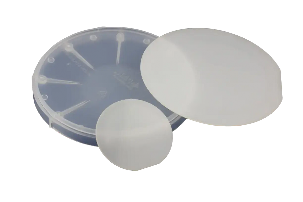
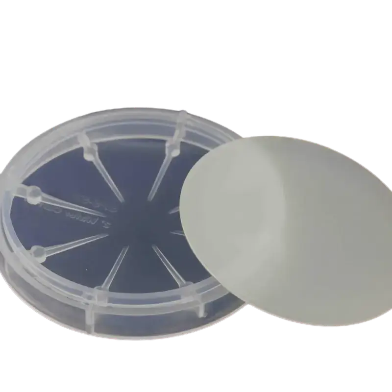
GaN on Sapphire wafer 4inch P GaN Gallium nitride Semiconductor Substrate
Size:4inch
Quantity:6 pieces
Quantity:
♦️High-quality GaN wafer for Research and Experiment.
♦️Provide small quantities, special specifications products, and customized services
♦️Global shipping, secure payment, large inventory.
♦️Minimum delivery time within 1 week. Shipped by FedEx, DHL,UPS, etc.
GaN on Sapphire Specification:
-
Sapphire Size: 4inch ;
-
Orientation: C-plane 0.2 +0.1° to M-plane;
-
Diameter: 100 mm±0.1 mm ;
-
Thickness: 650 ± 25 μm ;
-
Orientation Flat: A-plane +0.3°;
-
OF Length: 16 ±1 mm;
-
Front Side: CMP Ra ≤0.2 nm;
-
Back Side:Lapping (Ra: 0.6–1.2 µm);
-
Epi Structure
-
Layer 3: P‑doped GaN/Np > 3E16 / 0.5 µm
-
Layer 2: Undoped GaN ~1.5 µm
-
Layer 1: Buffer ~0.1 µm
-
Layer 0: Sapphire
-
Epi Thickness Total: 2.1 ± 0.3 µm;
-
Epi Thickness Std: <3%;
-
XRD
-
GaN (002):≤200 arcsec;
-
GaN (102):≤400 arcsec;
-
Carrier Concentration:3E16 cm⁻³ ;
-
Roughness: Ra <1.0 nm;
-
Production time: 4weeks;
Choose options
Size:4inch
Quantity:6 pieces
Quantity:
♦️High-quality GaN wafer for Research and Experiment.
♦️Provide small quantities, special specifications products, and customized services
♦️Global shipping, secure payment, large inventory.
♦️Minimum delivery time within 1 week. Shipped by FedEx, DHL,UPS, etc.
GaN on Sapphire Specification:
-
Sapphire Size: 4inch ;
-
Orientation: C-plane 0.2 +0.1° to M-plane;
-
Diameter: 100 mm±0.1 mm ;
-
Thickness: 650 ± 25 μm ;
-
Orientation Flat: A-plane +0.3°;
-
OF Length: 16 ±1 mm;
-
Front Side: CMP Ra ≤0.2 nm;
-
Back Side:Lapping (Ra: 0.6–1.2 µm);
-
Epi Structure
-
Layer 3: P‑doped GaN/Np > 3E16 / 0.5 µm
-
Layer 2: Undoped GaN ~1.5 µm
-
Layer 1: Buffer ~0.1 µm
-
Layer 0: Sapphire
-
Epi Thickness Total: 2.1 ± 0.3 µm;
-
Epi Thickness Std: <3%;
-
XRD
-
GaN (002):≤200 arcsec;
-
GaN (102):≤400 arcsec;
-
Carrier Concentration:3E16 cm⁻³ ;
-
Roughness: Ra <1.0 nm;
-
Production time: 4weeks;
Size:4inch
Quantity:6 pieces
Quantity:
♦️High-quality GaN wafer for Research and Experiment.
♦️Provide small quantities, special specifications products, and customized services
♦️Global shipping, secure payment, large inventory.
♦️Minimum delivery time within 1 week. Shipped by FedEx, DHL,UPS, etc.
GaN on Sapphire Specification:
-
Sapphire Size: 4inch ;
-
Orientation: C-plane 0.2 +0.1° to M-plane;
-
Diameter: 100 mm±0.1 mm ;
-
Thickness: 650 ± 25 μm ;
-
Orientation Flat: A-plane +0.3°;
-
OF Length: 16 ±1 mm;
-
Front Side: CMP Ra ≤0.2 nm;
-
Back Side:Lapping (Ra: 0.6–1.2 µm);
-
Epi Structure
-
Layer 3: P‑doped GaN/Np > 3E16 / 0.5 µm
-
Layer 2: Undoped GaN ~1.5 µm
-
Layer 1: Buffer ~0.1 µm
-
Layer 0: Sapphire
-
Epi Thickness Total: 2.1 ± 0.3 µm;
-
Epi Thickness Std: <3%;
-
XRD
-
GaN (002):≤200 arcsec;
-
GaN (102):≤400 arcsec;
-
Carrier Concentration:3E16 cm⁻³ ;
-
Roughness: Ra <1.0 nm;
-
Production time: 4weeks;
♦️High-quality GaN wafer for Research and Experiment.
♦️Provide small quantities, special specifications products, and customized services
♦️Global shipping, secure payment, large inventory.
♦️Minimum delivery time within 1 week. Shipped by FedEx, DHL,UPS, etc.
GaN on Sapphire Specification:
-
Size: 2inch ;
-
Mg-Doped;
-
Diameter: 50.8 mm±0.3 mm ;
-
Thickness/Thickness STD: 4.5 ± 0.5 μm / < 3% ;
-
Orientation of GaN: C plane (0001) off angle toward A-axis 0.2 ± 0.1°;
-
Orientation Flat of GaN: (1-100) 0 ± 0.2°, 16 ± 1 mm;
-
Conduction Type: P-Type;
-
Resistivity (300K):< 10 Ω·cm;
-
Carrier Concentration:> 1 x 1017 cm -3 (doping concentration of p+GaN ≥ 5 x 1019 cm -3);
-
Mobility: > 5cm2/V·s ;
-
Structure:~ 0.5 μm p+GaN/~ 1.5 μm p-GaN /~ 2.5 μm uGaN /~ 25 nm uGaN buffer/430 ±25 μm sapphire;
-
XRD FWHMs: (0002)<300 arcsec,(10-12)<400 arcsec;
-
Orientation of Sapphire: C plane (0001) off angle toward M-axis 0.2 ± 0.1°;
-
Orientation Flat of Sapphire: (11-20) 0 ± 0.2°, 16 ± 1 mm ;
-
Sapphire Polish: Single-side polished (SSP)/Double-side polished (DSP);
-
UseableArea:> 90% (edge and macro defects exclusion);
-
Wafer case ;